
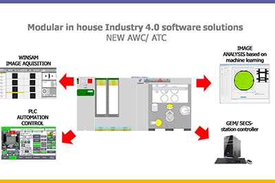
All PVA TePla SAM systems are controlled by an advanced, intuitive graphical user interface and the WINSAM 8 control program running on a Windows® 10 platform. WINSAM 8 is easy to learn and can be used for numerous tasks.
The program makes it possible to save and recall the device setup parameters with every image saved in TIFF format. All SAM parameters can be called up and reset, which allows the system to perform multiple analyses under identical conditions.
- More
Function overview:
- Adjustable amplification, gate width and gate delay before and during the scanning procedure
- Selectable threshold value, positive-negative peak-phase detection: amplitude, bipolar
- Completely flexible scanning field dimensions adjustable in the X and Y directions
- Flexible image resolution using selectable pixel size, configuration in the software
- Minimum pixel size 0.5 µm • Maximum resolution (32,000 x 32,000 pixels)
- Quick mode: Scanning with interpolation in the Y direction, e.g. with 500 x 250 resolution, can be applied to meander scan
- TIFF file contains multiple gate images
- SSP image display
- Flexible A-scan structure
- Visualization of the scanning field
- Complete remote connectivity
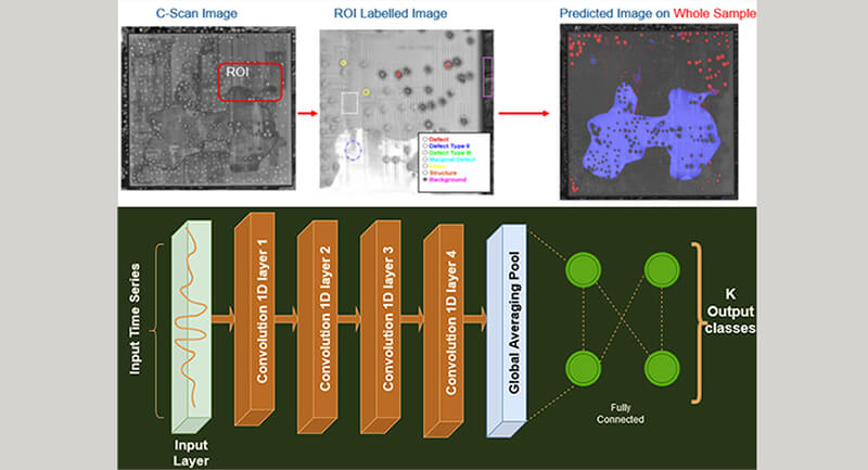
For specific customers and samples, PVA TePla can develop image-processing software that is tailored to the needs of our customers. It can be used to process images of wafers with and without chip structures.
- More
Function overview:
Image processing for wafers with chip structures
- Analyses using script language for specific chip structures
- Output of defects using wafer mapping (customer-specific formats are also possible)
Image processing for waters without chip structures
- Controlling the software using notch training
- Detection of defect size and position
- Inspection of the wafer edge

Our specific SECS/GEM interfaces provide the link between our systems and the connected production control system. They also enable the transfer of all production and system data, process values, and parameters.
This interface implementation meets the requirements of the SEMI Equipment Communications Standard (SECS) issued by the Semiconductor Equipment and Materials International (SEMI) industry association.
PVA TePla Analytical Systems GmbH has implemented SECS I, HSMS and Standard SECS II “Streams” and “Functions” for serial and TCP/IP communication with a host computer.

SAMnalysis combines state of the art pre- and post-processing algorithms with convenient results handling and a dedicated management system.
The software package was developed for the advanced failure analysis of SAM data, for quality control, and for scientific applications—for instance, in the areas of materials analysis, for biomedical problems, and for failure analyses in the semiconductor industry. Quantitative and qualitative evaluation routines and algorithms help to analyze recorded Z-scans.
- More
Function overview:
- 3D and volumetric investigation, of even the most complex samples
- 3D-rendering of internal structures and interfaces
- Evaluation of surface deformation (warpage, bow)
- Comprehensive evaluations and modifications of SAM data (image contrast, threshold, image interpolation, analytical image filtering)
- Time Of Flight analysis, thickness measurements using the duration of the ultrasound
- Toolbox for quantitative determination of mechanical and elastic properties
- Evaluation of broken areas
- Comparative image analysis of effects/defects/differences before and after stress
- Spectral and wavelet-based narrow-band imaging for resolution enhancement
- Quantitative analysis for extraction of defects or internal structures in the sample; various methods for accurately removing sample tilt